Symbolic examples
Introduction
A small signal symbolic analysis is requested through the .symbolic
directive.
Its syntax is:
.symbolic [tf=<source_name> ac=<bool> r0s=<bool>]
If the source is specified, all results are differentiated with respect to the source value, to obtain transfer functions.
If ac is set to 1, True or yes, capacitors and inductors
will be taken into account. If r0s is set to True or one of its
synonyms, the output resistances of the transistors will be considered.
See also
The symbolic analysis section in Netlist Syntax,
the module ahkab.symbolic and the helper function
ahkab.ahkab.new_symbolic().
Output resistance of a degenerated MOS transistor
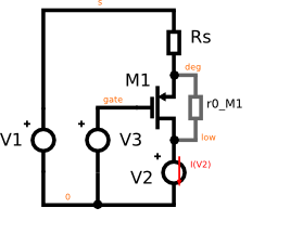
Let’s say we wish to check the expression of the output resistance of the circuit in the figure above, the small signal \(-\mathrm{V_2/I[V_2]}\).
Save the following netlist to a file, in the following the name of this file is assumed to be “rd.ckt”.
* Output resistance of a degenerated MOS transistor
m1 low gate deg 0 pch w=1u l=1u
rs deg s 1k
v1 gate 0 type=vdc vdc=1
v3 s 0 type=vdc vdc=1
v2 low 0 type=vdc vdc=1

.model ekv pch type=p kp=10e-6 vto=-1
.symbolic tf=v2 r0s=1
Start ahkab with:
./ahkab rd.ckt
Results
* OUTPUT RESISTANCE OF A DEGENERATED MOS TRANSISTOR
Starting symbolic DC...
Building symbolic MNA, N and x...  done.
Building equations...
Performing auxiliary simplification...
Auxiliary simplification solved the problem.
Success!
[ ... very long lines omitted  ... ]
Calculating small-signal symbolic transfer functions (v2))... done.
Small-signal symbolic transfer functions:
I_[V1]/v2 = 0
    DC: 0
I_[V2]/v2 = -1.0/(R_s*gm_M1*r0_M1 + R_s + r0_M1)
    DC: -1.0/(R_s*gm_M1*r0_M1 + R_s + r0_M1)
I_[V3]/v2 = 1.0/(R_s*gm_M1*r0_M1 + R_s + r0_M1)
    DC: 1.0/(R_s*gm_M1*r0_M1 + R_s + r0_M1)
V_deg/v2 = 1.0*R_s/(R_s*gm_M1*r0_M1 + R_s + r0_M1)
    DC: 1.0*R_s/(R_s*gm_M1*r0_M1 + R_s + r0_M1)
V_gate/v2 = 0
    DC: 0
V_low/v2 = 1.00000000000000
    DC: 1.00000000000000
V_s/v2 = 0
    DC: 0
The simulator solves the circuit symbolically and the differentiates the results according to the transfer function requested.
We wish to know the transfer function between \(V_2\) and \(-I[V_2]\), rearranging the results above:
Resistance seen at the source of a transistor with a resistor at the drain
Let’s evaluate the symmetric circuit to the previous one: this time the resistor is located at the drain (Rd) and we connect the test voltage source at the transistor source node.
We wish to verify the famous result:
Which evaluates to \(1/g_m\) if:
- \(g_mr_0 >> 1\),
- \(r_0 >> R_D\).
The circuit we wish to simulate to extract the equivalent resistance is:
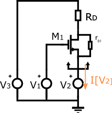
which can be described with the netlist:
* Resistance seen at the source of a
* transistor with a resistor at the drain
m1 low gate deg 0 pch w=1u l=1u
rd low s 1k
v1 gate 0 type=vdc vdc=1
v3 s 0 type=vdc vdc=2
v2 deg 0 type=vdc vdc=1

.model ekv pch type=p kp=10e-6 vto=-1
.symbolic tf=v2 r0s=1
Running ahkab just like in the example before, we get:
Starting symbolic AC analysis...
Building symbolic MNA, N and x...  done.
Building equations...
Solving...
Success!
Results:
I[V1]    = 0
I[V2]    = (V1*gm_m1*r0_m1 - V2*gm_m1*r0_m1 - V2 + V3)/(RD*(1 + r0_m1/RD))
I[V3]    = (-V1*gm_m1*r0_m1 + V2*(gm_m1*r0_m1 + 1) - V3)/(RD*(1 + r0_m1/RD))
Vdeg     = V2
Vgate    = V1
Vlow     = (-V1*gm_m1*r0_m1 + V2*(gm_m1*r0_m1 + 1) + V3*r0_m1/RD)/(1 + r0_m1/RD)
Vs   = V3
Calculating small-signal symbolic transfer functions (V2))... done.
Small-signal symbolic transfer functions:
I[V1]/V2 = 0
    DC: 0
I[V2]/V2 = (-gm_m1*r0_m1 - 1)/(RD + r0_m1)
    DC: (-gm_m1*r0_m1 - 1)/(RD + r0_m1)
I[V3]/V2 = (gm_m1*r0_m1 + 1)/(RD + r0_m1)
    DC: (gm_m1*r0_m1 + 1)/(RD + r0_m1)
Vdeg/V2 = 1
    DC: 1
Vgate/V2 = 0
    DC: 0
Vlow/V2 = RD*(gm_m1*r0_m1 + 1)/(RD + r0_m1)
    DC: RD*(gm_m1*r0_m1 + 1)/(RD + r0_m1)
Vs/V2 = 0
    DC: 0
Where the transfer function we are looking for is \(-V_2/I[V_2]\).
After rearranging, we get:
Just like it was expected.
Small-signal transfer function of various opamp configurations
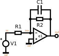
Integrator with finite gain
The ideal integrator is the configuration shown above with no \(R_2\) resistor. It has a transfer function equal to \(T(s) = K/s\) for all frequencies. Notice the infinite zero-frequency gain.
A real integrator will have a transfer function differing from the one above because of many factors. One of which is the finite gain of every amplifier. This goes well with the simulator as it does not like “infinite quantities”.
Netlist:
PERFECT INTEGRATOR
v1 in 0 type=vdc vdc=1
r1 in inv 1k
e1 out 0 0 inv 1e6
c1 inv out 1p

.symbolic tf=v1 ac=1
If the amplifier has a gain equal to \(e_1\), then, skipping to the results, we get:
I[E1]    = (C1*s*v1 + C1*e1*s*v1)/(1 + C1*R1*s + C1*R1*e1*s)
I[V1]    = -(C1*s*v1 + C1*e1*s*v1)/(1 + C1*R1*s + C1*R1*e1*s)
Vin  = v1
Vinv     = v1/(1 + C1*R1*s + C1*R1*e1*s)
Vout     = -e1*v1/(1 + C1*R1*s + C1*R1*e1*s)
Calculating symbolic transfer functions (v1)... done!
d/dv1 I[E1] = (C1*s + C1*e1*s)/(1 + C1*R1*s + C1*R1*e1*s)
    DC: 0
    P0: 1/(-C1*R1 - C1*R1*e1)
    Z0: 0
d/dv1 I[V1] = -(C1*s + C1*e1*s)/(1 + C1*R1*s + C1*R1*e1*s)
    DC: 0
    P0: 1/(-C1*R1 - C1*R1*e1)
    Z0: 0
d/dv1 Vin = 1
    DC: 1
d/dv1 Vinv = 1/(1 + C1*R1*s + C1*R1*e1*s)
    DC: 1
    P0: 1/(-C1*R1 - C1*R1*e1)
d/dv1 Vout = -e1/(1 + C1*R1*s + C1*R1*e1*s)
    DC: -e1
    P0: 1/(-C1*R1 - C1*R1*e1)
\(dV_{out}/dv_1\) is what we are interested in, here: the DC gain increases proportionally to \(e_1\) and the position of the low frequency pole moves back towards DC with \(e_1\) increasing.
Leaky integrator with finite gain
If we introduce a resistor \(R_2\) shunting the capacitor, we get a low frequency amplifier, which approximately behaves like an amplifier with constant gain \(-R_2/R_1\) before \(\omega = -1/(C_1 R_2)\), then the gain decreases by 20dB/decade.
Netlist:
LEAKY INTEGRATOR WITH FINITE GAIN
v1 in 0 type=vdc vdc=1
r1 in inv 1k
e1 out 0 0 inv 1e6
c1 inv out 1p
r2 inv out 1k

.symbolic tf=v1 ac=1
From the simulation:
I[E1]    = (v1 + e1*v1 + C1*R2*s*v1 + C1*R2*e1*s*v1)/(R1 + R2 + R1*e1 + C1*R1*R2*s + C1*R1*R2*e1*s)
I[V1]    = (v1 + e1*v1 + C1*R2*s*v1 + C1*R2*e1*s*v1)/(-R1 - R2 - R1*e1 - C1*R1*R2*s - C1*R1*R2*e1*s)
Vin  = v1
Vinv     = R2*v1/(R1 + R2 + R1*e1 + C1*R1*R2*s + C1*R1*R2*e1*s)
Vout     = R2*e1*v1/(-R1 - R2 - R1*e1 - C1*R1*R2*s - C1*R1*R2*e1*s)
Calculating symbolic transfer functions (v1)... done!
d/dv1 I[E1] = (1 + e1 + C1*R2*s + C1*R2*e1*s)/(R1 + R2 + R1*e1 + C1*R1*R2*s + C1*R1*R2*e1*s)
    DC: (1 + e1)/(R1 + R2 + R1*e1)
    P0: (R1 + R2 + R1*e1)/(-C1*R1*R2 - C1*R1*R2*e1)
    Z0: -1/(C1*R2)
d/dv1 I[V1] = (1 + e1 + C1*R2*s + C1*R2*e1*s)/(-R1 - R2 - R1*e1 - C1*R1*R2*s - C1*R1*R2*e1*s)
    DC: (1 + e1)/(-R1 - R2 - R1*e1)
    P0: (R1 + R2 + R1*e1)/(-C1*R1*R2 - C1*R1*R2*e1)
    Z0: -1/(C1*R2)
d/dv1 Vin = 1
    DC: 1
d/dv1 Vinv = R2/(R1 + R2 + R1*e1 + C1*R1*R2*s + C1*R1*R2*e1*s)
    DC: R2/(R1 + R2 + R1*e1)
    P0: (R1 + R2 + R1*e1)/(-C1*R1*R2 - C1*R1*R2*e1)
d/dv1 Vout = R2*e1/(-R1 - R2 - R1*e1 - C1*R1*R2*s - C1*R1*R2*e1*s)
    DC: R2*e1/(-R1 - R2 - R1*e1)
    P0: (R1 + R2 + R1*e1)/(-C1*R1*R2 - C1*R1*R2*e1)
If \(e_1\) is indeed very high, the circuit results are as expected.
Effects of finite output resistance, differential input capacitance, finite input resistance can all be simulated similarly.
